Samsung is a multinational manufacturing corporation headquartered in Samsung Digital City, Suwon, South Korea. The world’s largest producer of dynamic random-access memory chips, which are utilized in computers and smartphones.
Let’s read the news and find out more.
Samsung Unveils New Memory Chip With ‘Highest-Capacity to Date’ For AI
On Tuesday, the multinational company Samsung Electronics announced that it had created a new high-bandwidth memory chip and claimed it has the “highest capacity to date.”
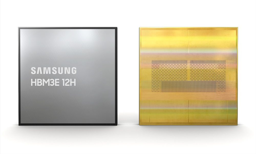
The company has created HBM3E 12H, the highest-capacity HBM product to date and the first 12-stack HBM3E DRAM in the industry.
This newly launched chip, HBM3E 12H, will provide a high bandwidth of up to 1,280 gigabytes per/sec (GB/s) and an industry-leading capacity of 36 gigabytes (GB) compared to the 8-stack HBM3 8H. These aspects have improved by more than 50%.
Yongcheol Bae, Executive Vice President of Memory Product Planning at Samsung Electronics, stated, “The industry’s AI service providers are increasingly requiring HBM with higher capacity, and our new HBM3E 12H product has been designed to answer that need,”
Also, read “AT&T Offers Full Day $5 Credit for Outage.”
He added, “This new memory solution forms part of our drive toward developing core technologies for high-stack HBM and providing technological leadership for the high-capacity HBM market in the AI era.”
The chipmakers continue to benefit from the AI boom. Generative AI models like OpenAI’s ChatGPT need several high-performance memory chips.
These chips allow generative AI models to produce human-like responses by remembering specifics from previous discussions and user preferences.

As many are experimenting with AI and people’s demands and interests are piqued towards the growing technological advancement, the AI markets are equally growing and benefitting.
The U.S. chipmaker Nvidia reported a 265% increase in revenue for the fourth fiscal quarter due to the rapid demand for its graphics processing units, which run and train ChatGPT.
Also, read “Google Launches Gemini AI for Workspace Tools at $20.”
Samsung Electronics stated, “As AI applications grow exponentially, the HBM3E 12H is expected to be an optimal solution for future systems that require more memory. Its higher performance and capacity will especially allow customers to manage their resources more flexibly and reduce total cost of ownership for data centers.”
“When used in AI applications, it is estimated that, in comparison to adopting HBM3 8H, the average speed for AI training can be increased by 34% while the number of simultaneous users of inference services can be expanded more than 11.5 times.”
Samsung said that although the HBM3E 12H has a 12-layer stack, it uses an innovative thermal compression non-conductive film that enables the 12-layer products to meet current HBM package requirements by having the same height specification as the 8-layer ones. To conclude, there are no changes in the physical dimensions of the chips, but only the chip’s processing capacity is increased.
The company claimed, “Samsung has continued to lower the thickness of its NCF material and achieved the industry’s smallest gap between chips at seven micrometers (µm) while also eliminating voids between layers.”
It added, “These efforts result in enhanced vertical density by over 20% compared to its HBM3 8H product.”
Also, read “Elon Musk: First Neuralink User Controls Mouse with Thoughts.”
To conclude, Samsung claimed that mass production of the HBM3E 12H is scheduled for the first half of 2024 and that the company has begun sampling the chip to customers.


Add Comment